1. Laser fine drilling & Printed Circuit Board (PCB)
The manufacturing industry is becoming more intelligent. This transformation and upgrading are driving the demand for advanced precision processing. This kind of processing has high added value and technical barriers. The demand for high-precision processing is on the rise. This has led to the rapid development of related fine-processing technologies. Laser fine processing technology is receiving increasing recognition and attention in the market. It is considered a highly-developed technology.
Laser fine drilling is a crucial component of laser fine processing. It is extensively used in the PCB industry. Laser-based PCB processing is rapid and can achieve an accuracy of 2μm. This level of precision is impossible with traditional equipment. Additionally, this technology can drill small, micro, and invisible holes. It fulfills the specific needs of the PCB market.
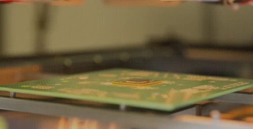
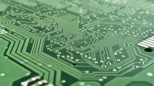
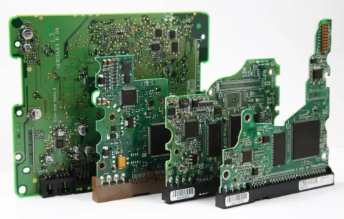
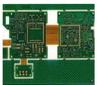
PCB, called printed circuit board, is an important device in the electronics industry. It is an important carrier for connecting components. It supports the development of the electronics industry. PCB is an indispensable part of most electronic gadgets. Laser fine drilling has become a common application in PCB manufacturing. The CO2 laser or ultraviolet laser is used to drill blind holes and through holes at high speeds. This results in high processing efficiency and desirable outcomes.
The PCB industry’s development has led to laser precision technology’s development. This brings more opportunities to the laser drilling industry.
2. The main applications of laser fine drilling in PCB
In recent decades, the manufacturing industry has continuously advanced. This has led to higher demands for circuit boards. It is due to the miniaturization and high-speed requirements of electronic products. The main goal is to make circuit boards smaller. This means reducing circuit width. It also means increasing the number of micro vias between circuit levels. Printed circuit boards have continuously shrunk in size while improving performance. They have evolved from single-layer to double-sided, multi-sided, multi-layer, and flexible boards. This evolution aims to achieve high density and high precision with small spacing. It also seeks to include micro-porous features and high reliability. As a result, the various functions’ pore sizes are also inclined to smaller diameters. This has helped develop smaller, faster circuit boards.
Currently, the PCB industry is progressing towards thinness, high integration, and high precision. The conventional production method often encounters problems. These include edge burrs, dust, stress, vibrations, and limitations in processing curves. However, laser technology has gradually emerged as a favorable solution for PCB manufacture. It uses non-contact processing, which doesn’t stress or deform the board. It also doesn’t generate dust and can process boards with components. Additionally, it has the flexibility to process any graphics.
In the PCB manufacturing process, drilling is very important. PCB boards also have high requirements for holes. Laser technology continues to advance. As a result, laser drilling is now essential for PCB production. An essential part.
3. Advantages of laser drilling:
In the field of laser processing, researchers and technicians in foreign countries have also noticed issues with micro-hole production and circuit board forming. Not just in China. Laser technology’s superior qualities have proven advantageous. They highlight the benefits of laser drilling over mechanical drilling. Laser beams have characteristics like high coherence, directionality, brightness, and monochromaticity. These characteristics make laser beams more energy-dense and faster. They also have less impact on non-exposed parts. As a result, the heat-affected area is minimized. This decreases the deformation caused by heating. The flexibility of laser beam processing is noteworthy. It allows for changes in direction, guidance, and focus. This can also be integrated with CNC systems for various workpieces. This improves processing quality and production efficiency, making it a highly convenient method.
In the PCB board production process, two laser technologies can be used for fine drilling:
- The wavelength of CO2 laser is in the far infrared band
- The wavelength of UV laser is within the ultraviolet band
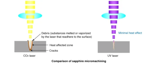
CO2 laser processing is currently a widely used laser processing method in PCB drilling. Its operating principle is this: CO2 gas can generate a practical pulsed infrared laser. This happens when the power is increased and the discharge time remains unchanged. It is penetrating and can penetrate most organic materials. CO2 lasers are used in the production of industrial micro-vias in printed circuit boards. The micro-vias’ diameter must be over 100 μm (Raman, 2001). Regarding the production of these large-aperture holes, CO2 laser has high productivity. This is because the punching time required for CO2 laser to make large holes is very short. Ultraviolet laser technology is widely used in the production of micropores with a diameter of less than 100 μm. With the use of micro circuit diagrams, the aperture diameter can even be less than 50 μm.
UV laser technology generally uses lasers for technical processing. The UV laser beam uses a process called “cold ablation”. This process reduces the heat-affected zone. It can eliminate the effects of edge processing, carbonization, and other thermal stresses. Minimize.
Applications that take advantage of the small beam size and low stress properties of UV lasers are drilling holes. This includes through holes, microvias, and blind and buried vias. UV laser systems drill holes by focusing a vertical beam to cut straight through the substrate. Depending on the material used, holes as small as 10 μm can be drilled.
UV lasers are especially useful for drilling multi-layer PCBs. The PCBs use composite materials that are hot-pressed and die-cast together. These so-called “semi-cures” can separate, especially after processing with hotter lasers.
UV laser technology has very high throughput when producing holes with diameters less than 80 μm. Therefore, in order to meet the increasing needs of micro-hole productivity, many circuit board manufacturers have begun to introduce double-head laser drilling systems.
Below are the three main types of dual-head laser drilling systems on the market today:
1)Double-head UV drilling system;
2)Double-head CO2 laser drilling system;
3) Combined laser drilling system (CO2 and ultraviolet light).
Drilling systems in HDI PCB board manufacturing have their own set of pros and cons. Laser drilling systems can be categorized into two types. The first type has a single wavelength and uses dual-drill bit systems. The second type uses dual wavelengths and dual-drill bit systems.
Regardless of the type, two key factors impact the ability to drill:
1) Laser energy/pulse energy;
2) Beam positioning system.
The energy of the laser pulse and the beam’s transmission power impact the time of laser drilling. The beam’s transmission power refers to the time required by the laser drilling machine to create a micro-through hole. The beam positioning system plays a crucial role in determining the movement speed between two holes. Together, these factors determine how quickly a laser drill can create the microvias required for a given need. For high aspect ratio integrated circuits, holes smaller than 90μm are necessary. Dual-head UV laser systems are the most appropriate. The double-head CO2 laser system uses a Q-switched, radio frequency-excited CO2 laser. It offers multiple benefits. These features include high repeatability (up to 100kHz). In addition, it has a wide operating surface and quick drilling. While it requires only a few shots to drill a blind hole, the drilling quality may not be optimal.
4. Conclusion
Advances in integrated circuits and electronic information technology have revolutionized the printed circuit board industry. This progress has also had a significant impact on the field of laser technology. As a result of constant innovations, it is now possible to produce electronic gadgets that are compact, versatile, and efficient. However, with these high standards comes an increased demand for precise PCB circuit board processing equipment.
Notably, laser technology has become an essential feature of PCB circuit board manufacturing. The growth of laser technology directly correlates to the development of PCB circuit board technology. By providing accurate component placement and ensuring high-quality and safety standards, laser technology has dramatically improved PCB assembly precision. In conclusion, the progress in integrated circuits and electronic information technology has led to significant changes in PCB circuit board technology, while the advancements in laser technology have added speed, precision, and accuracy to the manufacturing process. Therefore, laser technology is an integral part of the printed circuit board industry.